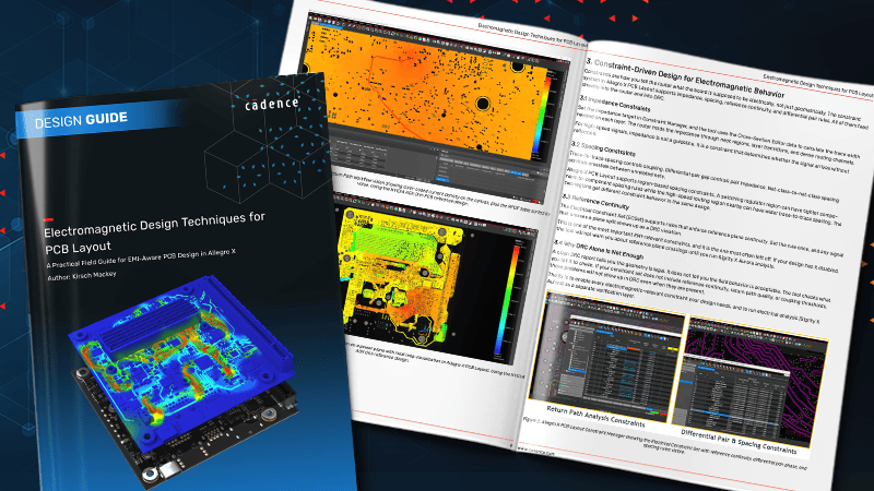
Electromagnetic Design Techniques for PCB Layout
Topics Covered
- EMI-Aware PCB Layout & Routing
- Signal Integrity & Return Path Design
- PCB Stackup & Impedance Control
- Power Distribution & Decoupling
- Crosstalk, Coupling & Shielding Techniques
- Pre-Compliance EMI Validation
Guide Overview
Electromagnetic interference (EMI) issues are rarely caused by individual components. More often, they originate from PCB layout decisions such as poor return paths, excessive loop areas, inadequate power distribution, signal coupling, and stackup choices. This practical design guide explains how electromagnetic behavior is established during layout and routing, helping engineers address EMI challenges before they result in costly failures, redesigns, or compliance testing delays.
Inside, you’ll learn proven techniques for creating EMI-aware PCB designs, including constraint-driven design methods, stackup and impedance planning, return path management, shielding strategies, power distribution network (PDN) optimization, and routing practices that reduce emissions.
Whether you’re developing high-speed digital systems, mixed-signal boards, power electronics, or other EMI-sensitive designs, this guide provides practical techniques to help you identify issues early, improve reliability, and reduce board respins. For more information on advanced PCB design, signal integrity, power integrity, and EMI-aware layout workflows, visit the Allegro X product page and discover how Cadence helps engineers design with confidence.
Thank You For Your Interest
By clicking ‘Submit’ you agree to our Terms of Use. We take your privacy seriously. For more information please read our Privacy Policy. By registering with All About Circuits you will automatically receive our weekly Product Update and Technology Insider eNewsletters.