
Passing EMI Compliance Testing the First Time: The Physics of Low-Emissions PCB Design
Topics Covered
- EMI Compliance Testing
- PCB Layout Best Practices
- High-Speed PCB Design
- Signal Integrity and Interference Reduction
Technical Article Overview
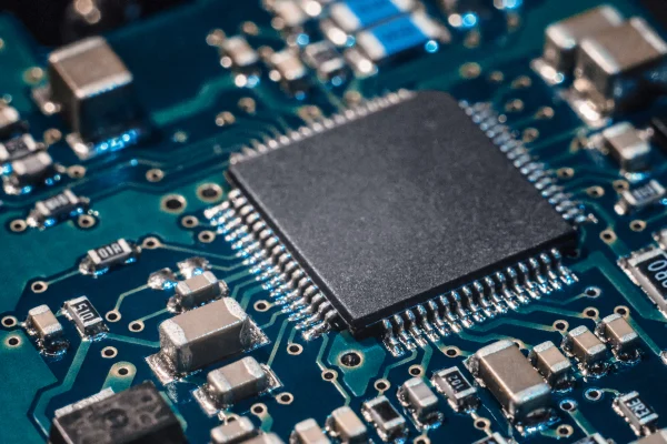
Any product designed today that requires high speed clocks can be troubled with electromagnetic compatibility (EMC) compliance issues. This technical article from Analog Devices outlines an electromagnetic (EM) field-oriented perspective for printed circuit board (PCB) design intended to help the reader pass electromagnetic interference (EMI) compliance testing the first time. The same techniques used for reducing EMI will also mitigate interference, suggesting a universal PCB layout philosophy. This article is presented in five parts. The first article covers the essential physics needed to understand why the techniques described within this article will mitigate EMI on a PCB layout. Part 2 will cover how the material in Part 1 plays into a practical board layout described through examples. Part 3 will discuss PCB layout strategies for complex boards that will satisfy the presented solutions. Part 4 will cover power routing and stack-up planning, while Part 5 will address specialized layout requirements.
Download now to see how the principles mentioned in Part 1 translate into three actionable layout practices that can help engineers design lower-emission boards and reduce the risk of costly compliance issues later in development.