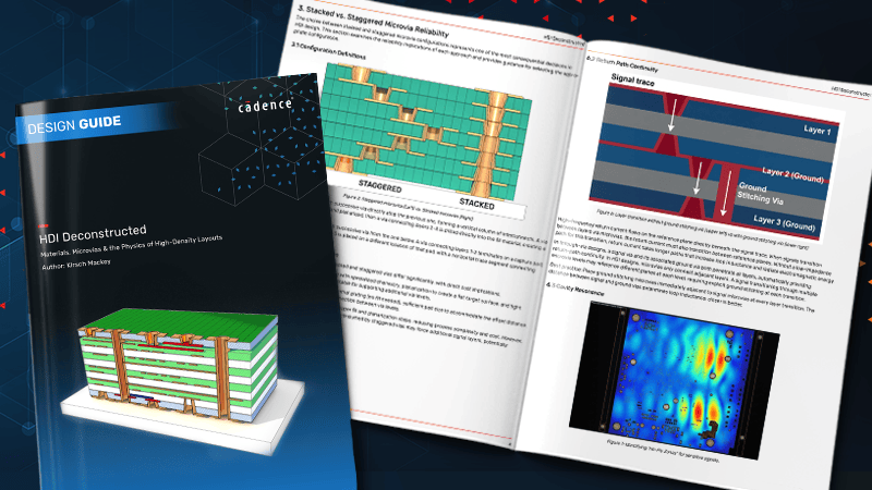
HDI Deconstructed
Topics Covered
- HDI Stackup Strategies
- Material Selection for HDI
- Microvia Design & Reliability
- PCB Manufacturability & Fabrication Risks
- Signal Integrity, Power Integrity & EMI
- Thermal Management in HDI Designs
Guide Overview
As electronic devices become smaller, faster, and more complex, High-Density Interconnect (HDI) technology has become a critical enabler of modern PCB design. This guide explores the key design and manufacturing considerations behind HDI, helping engineers balance performance, reliability, and manufacturability. Topics include microvia design and reliability, stackup optimization, material selection, signal integrity, power integrity, and EMI performance.
This guide also examines stacked versus staggered microvias, thermal management, fabrication constraints, cost tradeoffs, and common manufacturability risks. Learn proven best practices for reducing design challenges, improving yield, and maximizing board density without compromising performance.
Download the design guide to discover how HDI technology can help you optimize routing density, enhance signal integrity, improve product reliability, and successfully deliver next-generation electronic designs. For more information on how to design and validate advanced HDI PCBs, visit the Allegro X product page and discover how Cadence helps engineers design with confidence.
Thank You For Your Interest
By clicking ‘Submit’ you agree to our Terms of Use. We take your privacy seriously. For more information please read our Privacy Policy. By registering with All About Circuits you will automatically receive our weekly Product Update and Technology Insider eNewsletters.